WELCOME TO
GERRY'S ULTIMATE VHDL PONG TUTORIAL
VGA Interfacing and Control using MENTOR GRAPHICS "HDL DESIGNER" Software
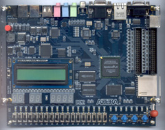
and the "Altera DE1" Development Board.

(SEE MY DEVOTED DE1 PAGE AT THE LINK BELOW)
http://www.digital-circuitry.com/MyLAB_IC_PROG_DE1.htm
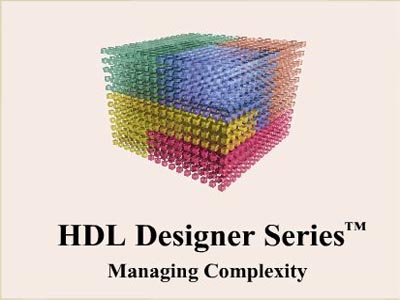
The Software used in this tutorial is called "HDL Designer" by Mentor Graphics, along with the Various companion programs such as
"ModelSim" and "Precision Synthesis".
If you are new to VHDL programming, I recommend that you review my "VHDL" page as an Introduction.
-= VHDL =-
However, if you are already programming and understand VHDL to some degree then you can skip the Intro and move on ahead.
-= Companion Textbook for this Project=-
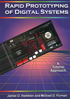
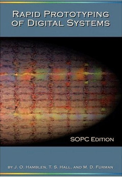
A highly recommended Textbook for this project is one of the two books shown Below:
"RAPID PROTOTYPING OF DIGITAL SYSTEMS"
These particular textbooks contain a great deal of information on VGA interfacing and it provides some of the Basic VHDL code for creating a VGA controller. I highly recommended that you purchase one of these books to help solidify your understanding.
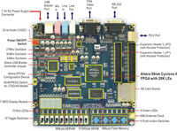
This Tutorial will show you how to program the Altera DE1 Development Board, to produce the required VGA control and data signals for displaying 2D color graphics on a VGA Computer Monitor. This in turn, will allow you to produce a basic 2D PONG style Video Game.
Many VHDL PONG style games have been demonstrated online. Such as this one below. This is similar to what your final project will look like once completed. However you are free to add more features to the game if you have the time to do so before the end of your Semester.
Additional features that you can add to your Game for those of you who wish to go beyond the outline of this Tutorial. Features such as a Score Board, Time Limit, Sound Effects, or even a Joystick/Game pad Control Interface for two players.
This is definitely Encouraged as it will help solidify your Understanding of the VHDL code.
This Tutorial uses a screen resolution of (640 x 480) with a 60Hz screen refresh rate. If you want to go all out and attempt to use higher Resolution settings such as (800 x 600), (1024 x 768) or even (1600 x 1200) then by all means do so. You would definitely be up for some major bonus points. :)
This Tutorial can easily be applied to other Development Boards and other VHDL software packages.
Boards such as The Altera DE2, Altera UP1,UP2, CPLDT-2 and Many more. You can even use a Universal Programmer to Program your own CPLD or FPGA. There is also the option of using a JTAG interface Programmer and wiring it up yourself to a JTAG compatible FPGA. This allows you to use a $15.00 JTAG programmer like the Altera "USB-BLASTER" to program your own "Off-the-Shelf" CPLD or FPGA. As long as the FPGA you purchase, supports a JTAG interface; then you can wire it up yourself and simply Program it with the same Logic Software you use with your DE1 development board.
Pretty Awesome!!
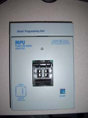

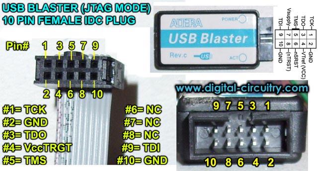
For a detailed explanation on the JTAG interface, Check out my "JTAG Interface" Page and Instructional Video at the Link Below:
http://www.digital-circuitry.com/MyLAB_IC_PROG_JTAG_ISP.htm
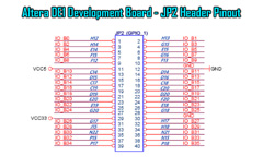
I have prepared a set of Instructional Videos for this project for your review. The videos will cover the concepts needed for you to combine 10 separate VHDL BLOCKs in HDL Designer, to produce a PONG Style Video Game on your Altera DE1 Development Board. You will Interface your DE1 to a VGA monitor using the onboard DB-15 VGA port.
Now, as this is a popular TERM Project for many Colleges and Universities... I will NOT be providing VHDL Source Code files for you to just download, copy and paste into your project and then submit it to your professor and get a free ride for this Project.
I will have various Instructional videos that will go over the fundamental concepts of the project; and I will also have some general VHDL "ARCHITECTURE" Examples for each of the 10 VHDL blocks. It will be up to you to apply the example to your own code. I believe it is important that you write out your own code, run simulations and see how things work through trial and Error.
Just Remember...You can do this !!
Try writing out some code yourself, run MultiSim simulations and you will see how quickly you can learn.
So again, I will NOT be giving out the VHDL source code files for download.
If you use this webpage and my Instructional Video's as a Guide, You will do just fine! :)
You can do this !!
Now, if I were to answer the 100's of e-mails you all send me, asking for help with your VHDL code, I would not be able to find the time to work or even eat. :) So please Register, and ask all of your VHDL questions on the edaboard.com CPLD/FPGA Digital Design Forum.
http://www.edaboard.com/forum30.html
If you need some help with your VHDL code or other Engineering related projects...the edaboard.com forum is the place to go. You can talk with other Professionals in the industry to help troubleshoot and solve your VHDL coding issues. Their Forum web-based GUI is outfitted with both "CODE" and "COMMENT" formatting. This makes your Message posts very clear and organized. Having your message posts clearly formatted this way, allows others to assist you more efficiently and in a timely manner. So this is a Fantastic resource and I highly recommend that you join.
Let's Get Started !!
The VGA Interface
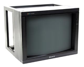
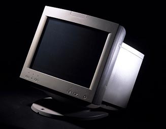
The VGA interface was Standardized in 1987 with signal requirements to display color images on a Cathode Ray Tube computer Monitor or (CRT) for short. When LCD monitors were later released, they adopted the same VGA signal standard in order to function with the current computer infrastructure out in the world.
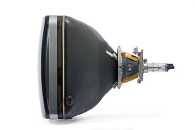
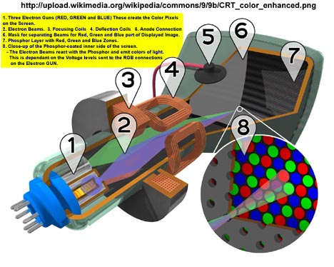
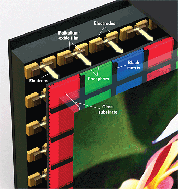
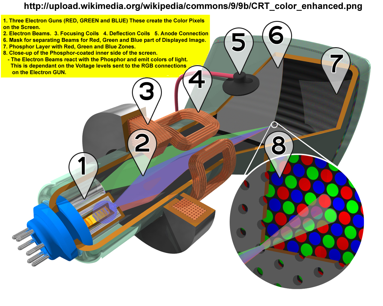
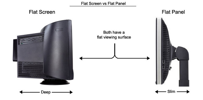
CRT - Cathode Ray Tube
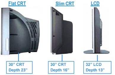
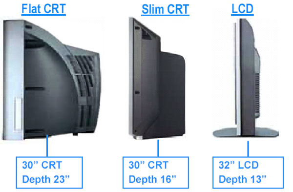
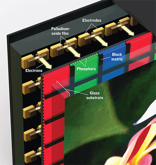
CRT & LCD Differences
CRT & LCD - Cutaway Diagram
Therefore LCD Monitors have an internal translator circuit that converts VGA Signals to the required Liquid Crystal display control Signals. This all happens automatically inside the LCD Monitors circuitry and it works all the same to us. So we don't have to worry about it.
We're Good to Go!
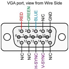
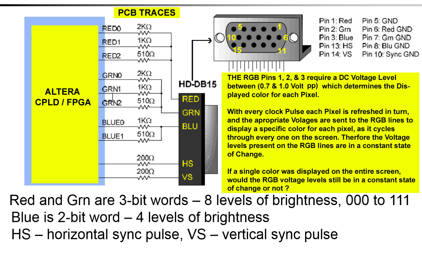
The VGA Interface - Signal Requirements
Basically there are 5 separate signal requirements for the VGA interface to function. These are H-SYNC & V-SYNC resolution control signals and the RED, GREEN and BLUE color display signals.
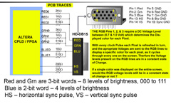
The H-SYNC & V-SYNC signals you send to the monitor, dictate which Resolution setting you are attempting to use. Depending on the monitor, it may only support a specific resolution, where other Monitors may support more than one. The Monitor stores reference signal Patterns for all of the available resolution settings, within an EEPROM memory chip that is part of the monitors internal circuitry.
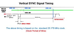
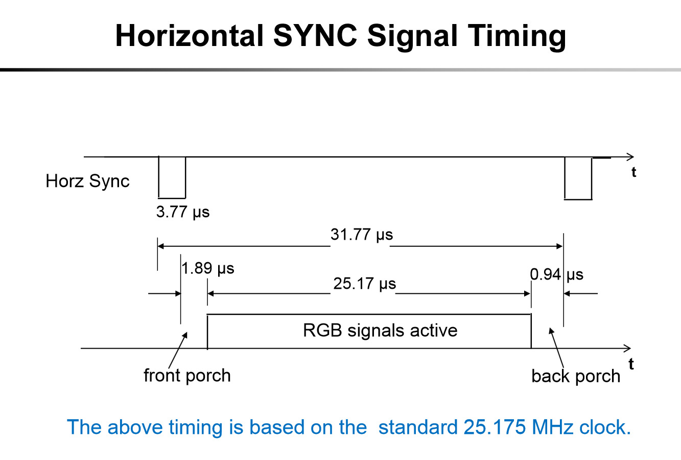
Each resolution setting requires a specific H-SYNC & V-SYNC frequency Pulse width, and Duty Cycle. These signal requirements have been Standardized by the Industry. We will be using the oldest and smallest screen resolution size available, as most VGA monitors will support it.
That being the VGA 640 x 480 Resolution with a 60Hz Refresh Rate.
The RED, GREEN and BLUE color control signal lines, each use Analog Voltage levels between (0.0 to 0.7 Volts DC) to determines the amount of color intensity used for each Pixel. As you know, all colors are made up from mixing various amounts of RED, GREEN and BLUE together. If this is confusing to you right now, don't worry we will come back to this again.
H-SYNC & V-SYNC Pulse Signals
I will try to explain this in Layman terms and offer you a different way of looking at these signals and how they work. Now this is just for the sake of explanation, so hopefully it will help you understand a little better.
Essentially the best way to understand what's happening here, is to view the H-SYNC and V-SYNC signals as Custom CLOCK Pulses that are constantly running and counting up to their MAXIMUM declared value, resetting to zero and then counting up once again. Every time the H-SYNC counter resets to zero, the V-SYNC counter is incremented only by 1. These counting sequences are repeated over and over again. These so called counters are basically our Horizontal and Vertical scanning lines.
Use the animated GIF Image shown below to see how the H-SYNC & V-SYNC signals are used to count through the Pixels on the screen from the Top Left corner all the way down in sequence to the Bottom Right corner. This process repeats 60 times per second, due to the fact that we are using a 60Hz refresh rate.
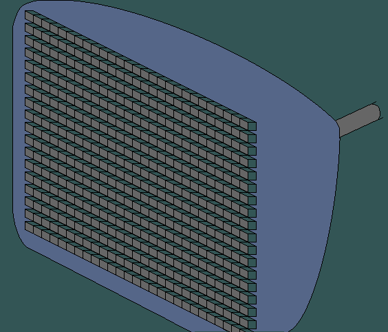
The Image above is actually showing what's called Interlaced Frames. You don't really need to worry about that right now, as we are not using this particular format. The animated image is mainly being used to show you the basic concept of a screen "Refresh Cycle".
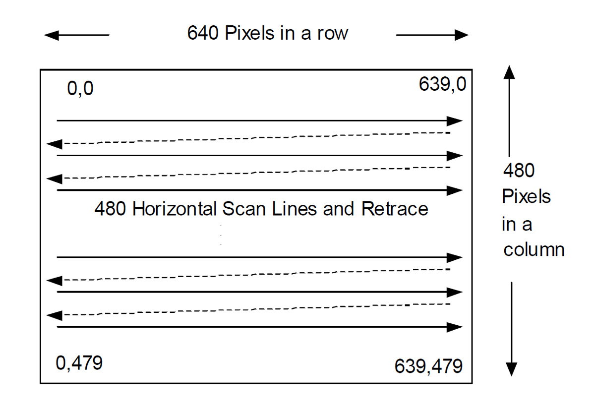
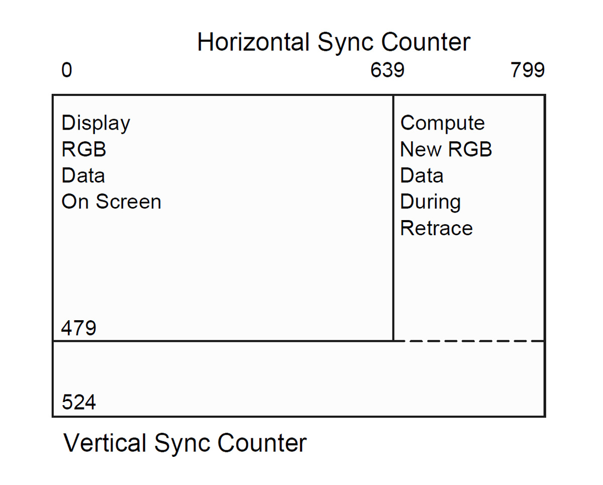
Now the fact that we are using a resolution setting of (640 x 480) this means that we have 640 Pixels that run from the left side of our screen to the Right Side. This also means that we have 480 Pixels that run from the Top of the screen to the Bottom.
In other words, what we have here is a 640 X 480 Pixel Matrix.
You can consider the Top Left corner of the Screen as the starting point for your H-SYNC counter. The H-SYNC Counter then proceeds to count through all 640 pixels on the first horizontal row from Left to Right. Once it reaches the end of the Row, it then resets to the beginning. However this time, it also moves down by one pixel to the next Row and increments the V-SYNC counter by 1.
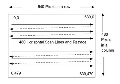
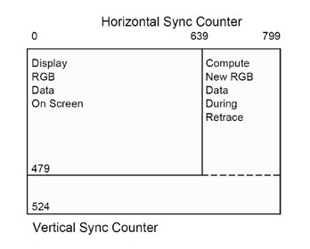
This process is repeated until the V-SYNC counter counts to 480, which brings it to the last Row at the Bottom of the screen. Then, when the H-SYNC counter reaches the last pixel on the Bottom Right corner of the Screen, both the H-SYNC and V-SYNC counters are reset to Zero.
This brings us back to the Top Left corner pixel and the entire counting Process starts all over again.
A single pass is called a "Refresh Cycle" and this is repeated 60 times per second to refresh the screen and update each pixel for a particular color and in turn, this produces an Image on the screen.
Review the Animated GIF image above to get a better understanding of this "Screen Refresh" process in action.
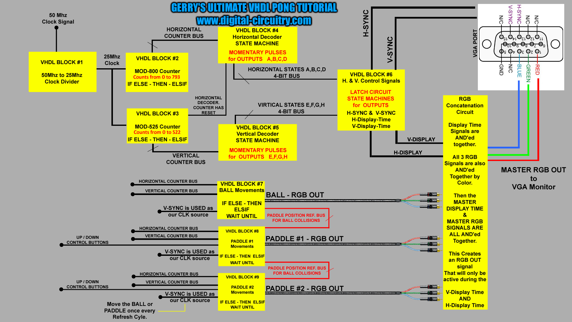
-= Overview of our 10 Block VHDL Circuit =-
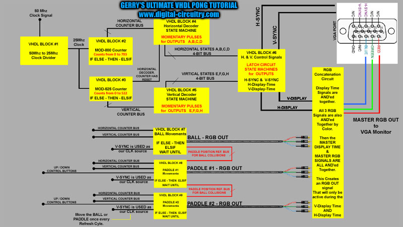
-= VHDL BLOCKS - Architecture Examples =-
Below I have provided some VHDL "Architecture" examples similar to what you would need for each of the 10 VHDL Blocks to perform their specific function. It is up to you to figure out how to apply the code to your own project, and generate the signals you need.
VHDL BLOCK #1 - The Clock Divider
The clock divider should be a snap for you to figure out so no real need for an example. For our VGA project we require a CLOCK signal of 25.175 MHz. 25 MHz in our case is fine. And we accomplish this by dividing the DE1 boards 50Mhz Clock signal by half.
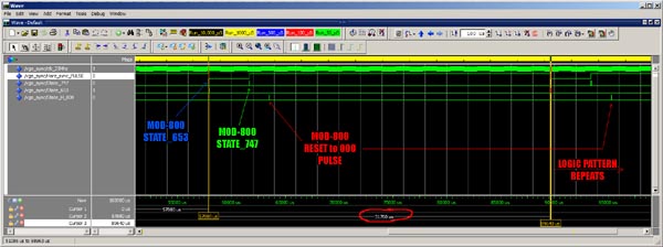
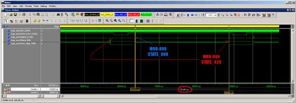
VHDL BLOCK #2 & #3 - A typical MOD Counter Example
(My MOD_25 Counter with a Power ON Reset line, and a 25Mhz Clock)
Single MOD Counter Example Example
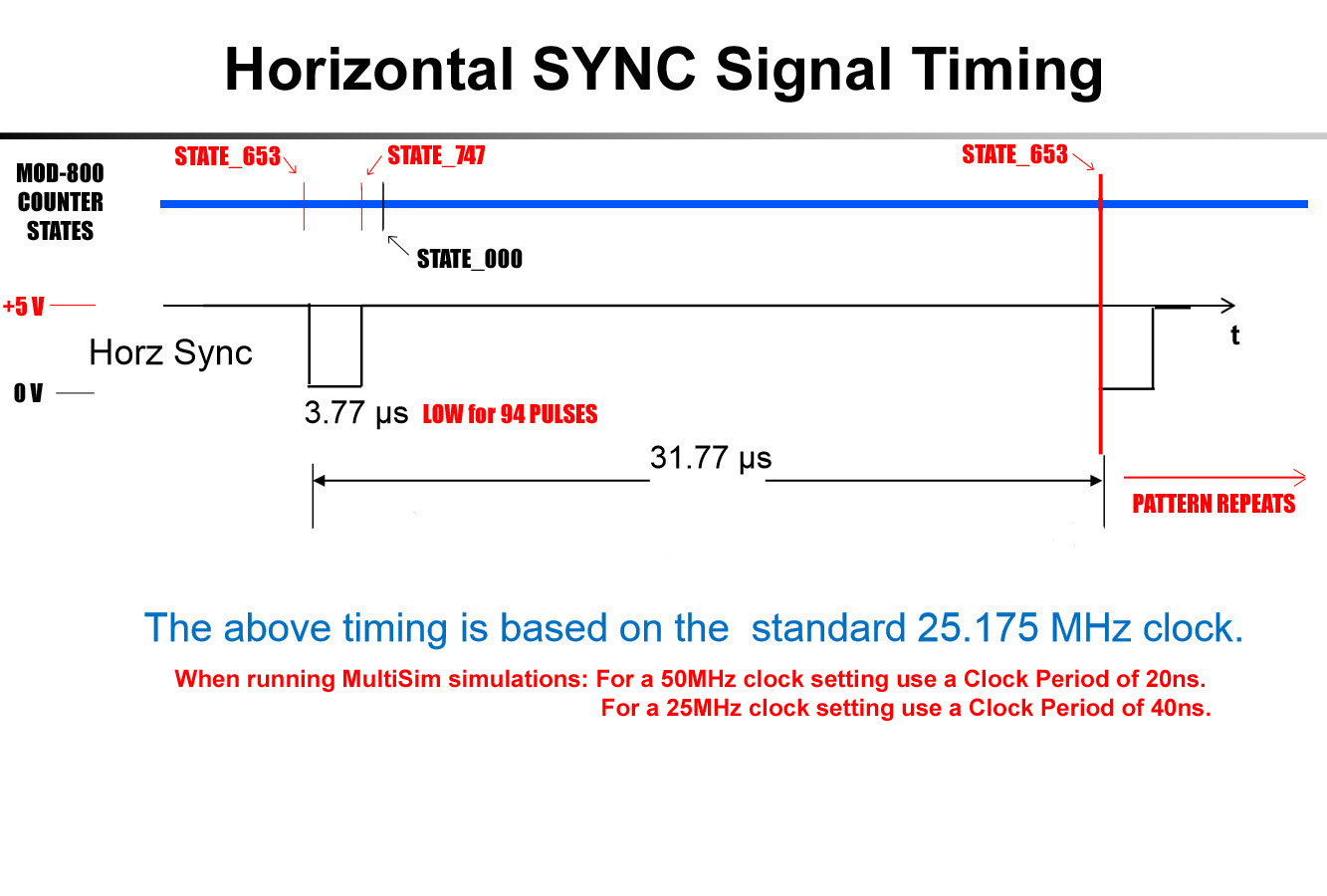
VHDL BLOCK #4 & #5 - The Horizontal & Vertical Decoder State Machines
(MOMENTARY PULSES FOR OUTPUT LINES)
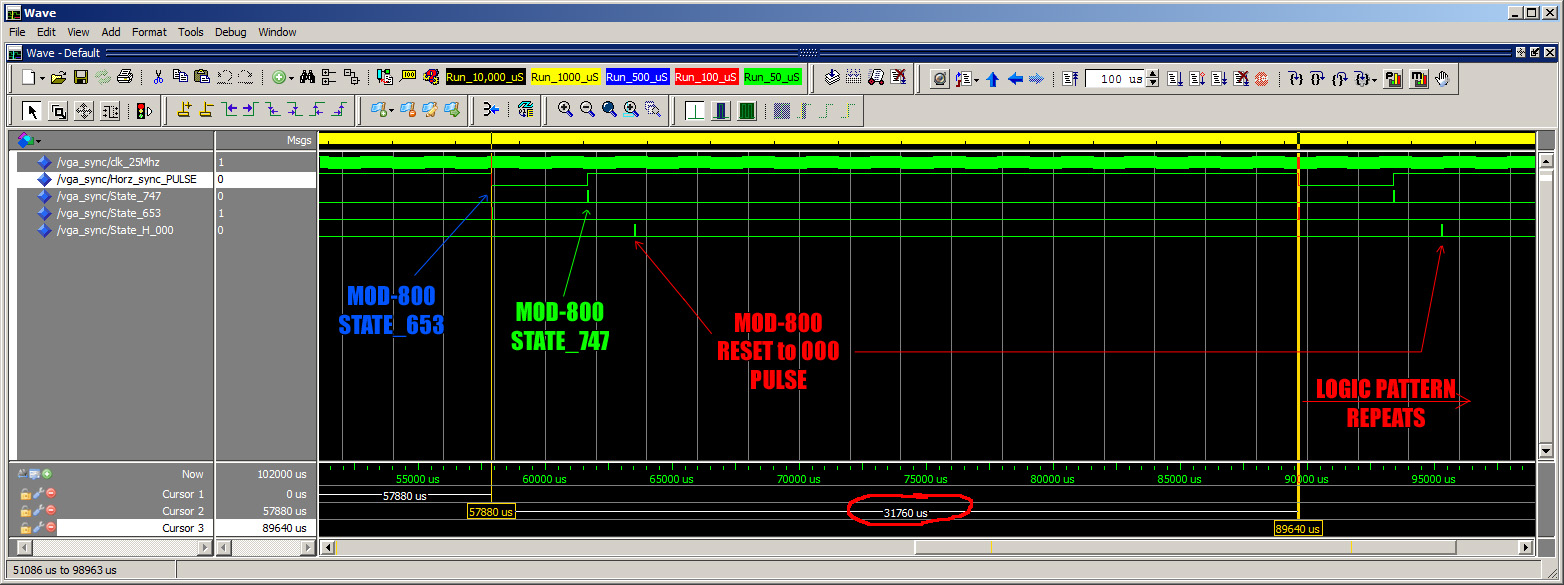
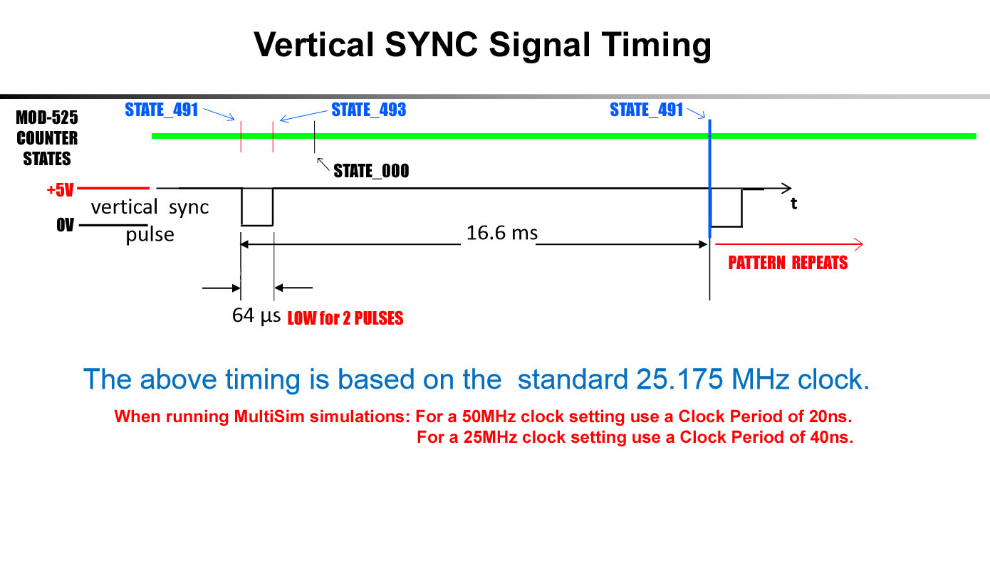
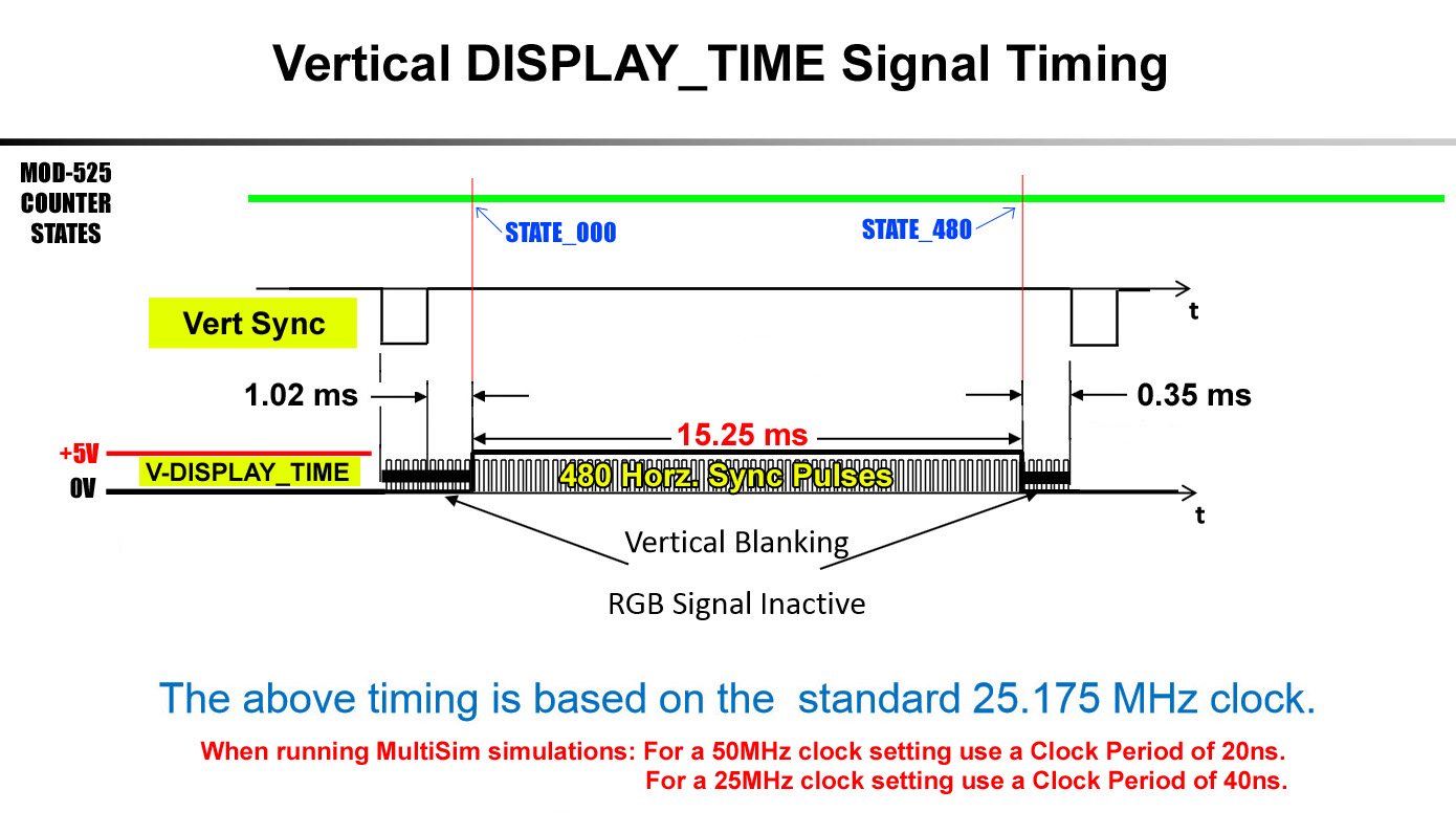
Be aware that this particular VHDL State machine will only create Momentary Logic High Pulses on your outputs. The output STATE_ lines will remain HIGH for only 1 Clock Pulse, based on the input CLK source used for this particular VHDL Block.
(The STATE_outputs need to be fed into a "Latch" circuit to be held HIGH for any length of time.)
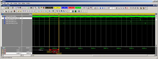
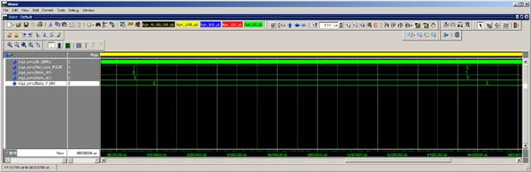
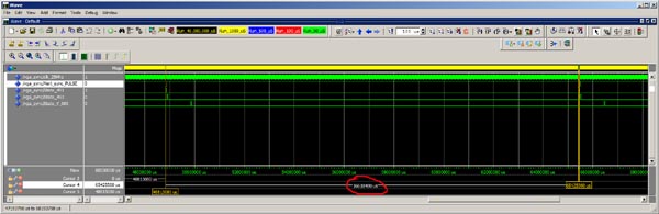
Single State Machine Example
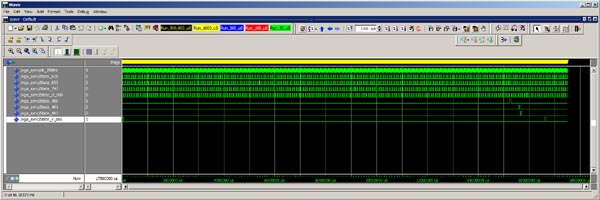
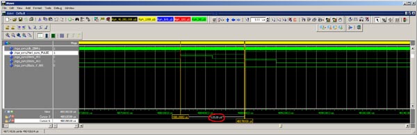
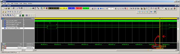
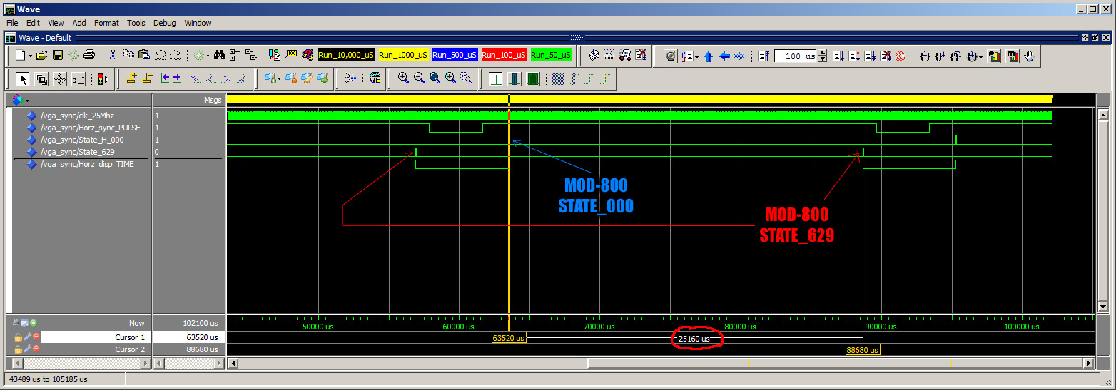
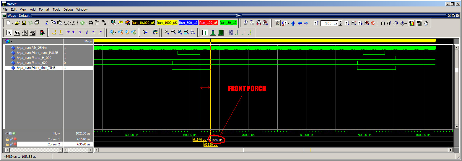
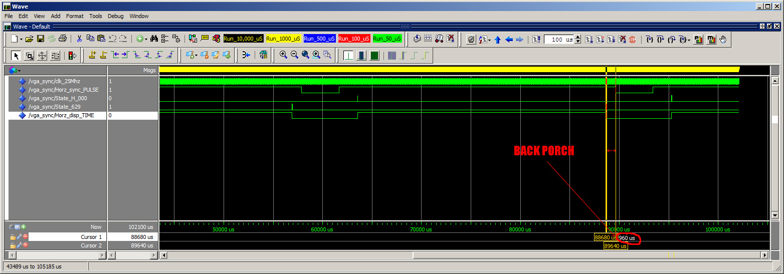
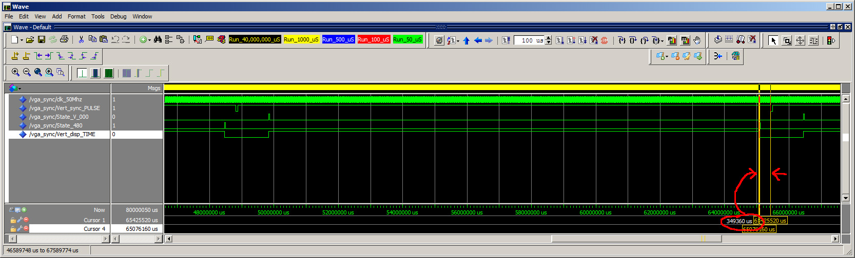
Above are some examples of various counter State Pulses.
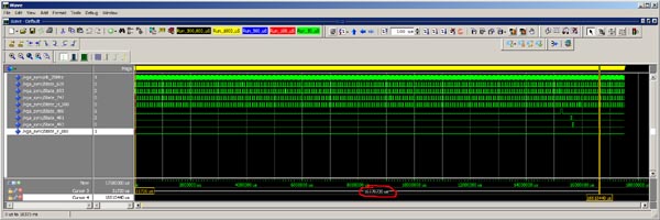
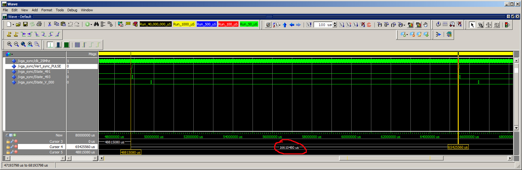
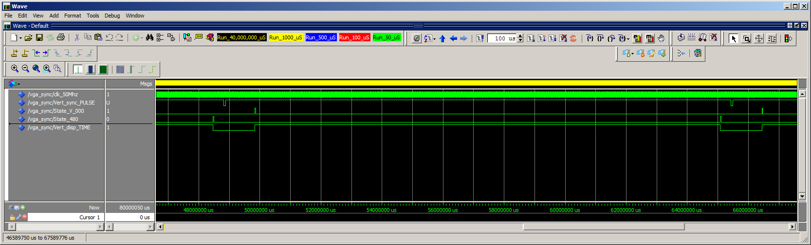
In the screen Capture shown above, Pay close attention to the time difference between the two Markers,
and how they relate to the other States Shown.
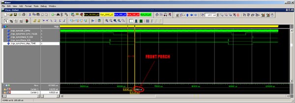
The Horizontal & Vertical "SYNC" & "DISPLAY_TIME" Signals
(LATCH CIRCUIT STATE MACHINES)
-= Horizontal "SYNC" Signal Timing Waveforms=-

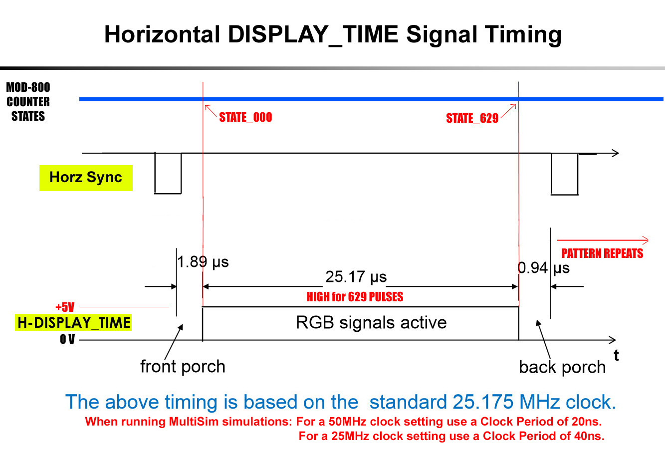
-= Horizontal "DISPLAY_TIME" Signal Waveforms =-
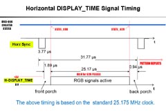
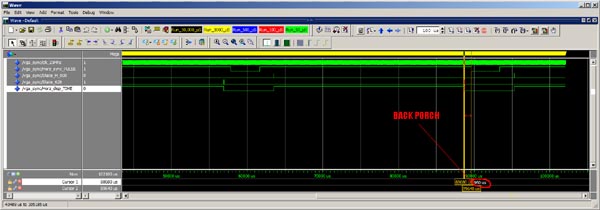
-= Vertical "SYNC" Signal Waveforms =-
-= Vertical "DISPLAY_TIME" Signal Waveforms =-
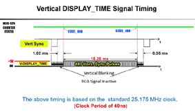
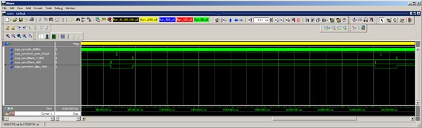
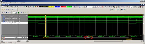
(LATCH CIRCUIT STATE MACHINES)
The VHDL Code below is an Example of a "Latch" circuit that will activate an output signal to remain either HIGH or LOW for any length of time until the output in question is assigned to change its state. Input Pulses are used to as Triggers to initiate any changes. This is essentially the type of circuit that you need to implement for each of the signals shown in the above Waveform diagrams.
Displaying Objects on the Screen
Now things do get a little more complicated here. I will have a couple of "DISPLAY PROCESS" examples to guide you along the way, however it is up to you to figure out how to add the Movement controls to your objects. :)
The best way to understand how basic colored objects are displayed on the screen is as Follows:
Try to look at the Horz. and Vert. MOD counters, more like an (X & Y) 2D coordinate system on a Map.
So envision our Horz. and Vert. MOD counters like the X & Y position coordinates for a Flashlight that is scanning the screen. This Flashlight is checking Labels on every pixel it comes across. The Labels indicate which color that particular Pixel should display. Red, Green or Blue, or any combination of the three.
The way we do this in VHDL is to use an additional set of std_logic_vectors or (COUNTERS) just like that used to generate the H-SYNC and V-SYNC signals. These Counter Pairs become the (X & Y) Reference coordinates for a single object that we display on the screen. This means that we will need an (X & Y) Counter pair, for each separate object that we have on the Screen.
So, as our Horz. and Vert. MOD counters are running through the screen Refresh cycle, if at any point the counters happen to have the exact same X and Y coordinates as one of the New (X & Y) Counter Pairs.......:
(Y_REFERENCE_COUNTER = V-COUNTER ... "AND".... X_REFERENCE_COUNTER = H-COUNTER)
then we can use this condition to activate the RGB lines to display a particular color "STARTING" from those (X & Y) coordinates. This means that you have to ADD the number of (X & Y) pixels to your Statement, in order for them to be displayed. Because you have essentially only told the system where to start painting the colors but not actually where or which way to go and where to stop.
(Y_REFERENCE_COUNTER = V-COUNTER ... "AND".... X_REFERENCE_COUNTER = H-COUNTER + size)
There is still a little more to it, so review the examples I have provided below, and see if you can figure it out. :)
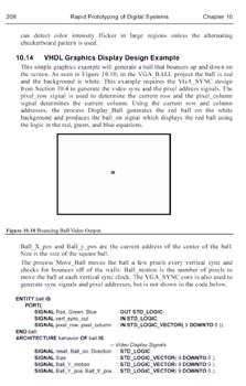
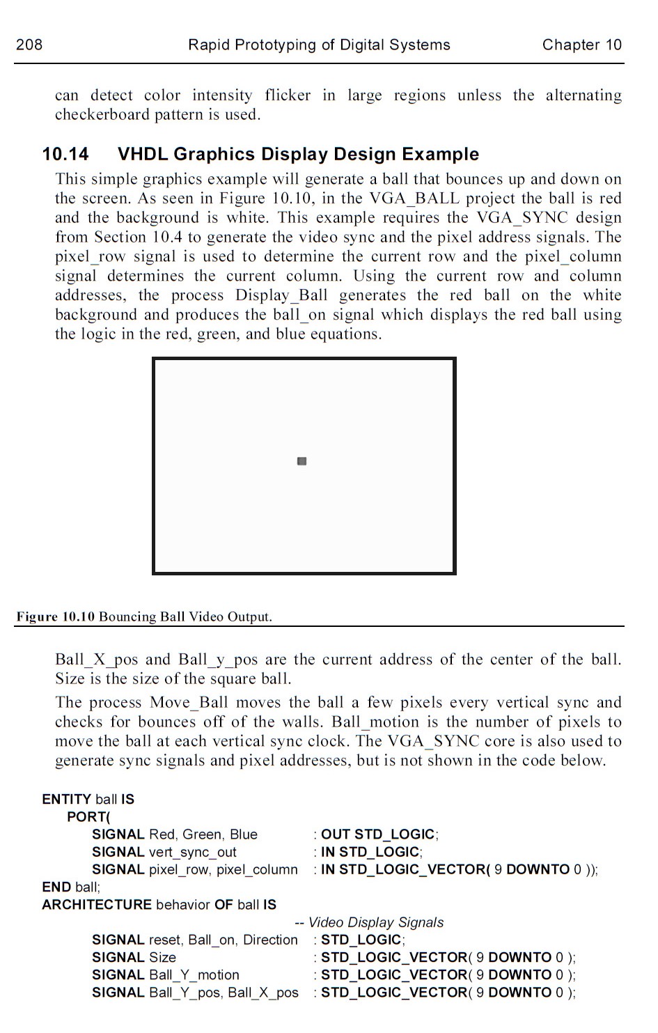
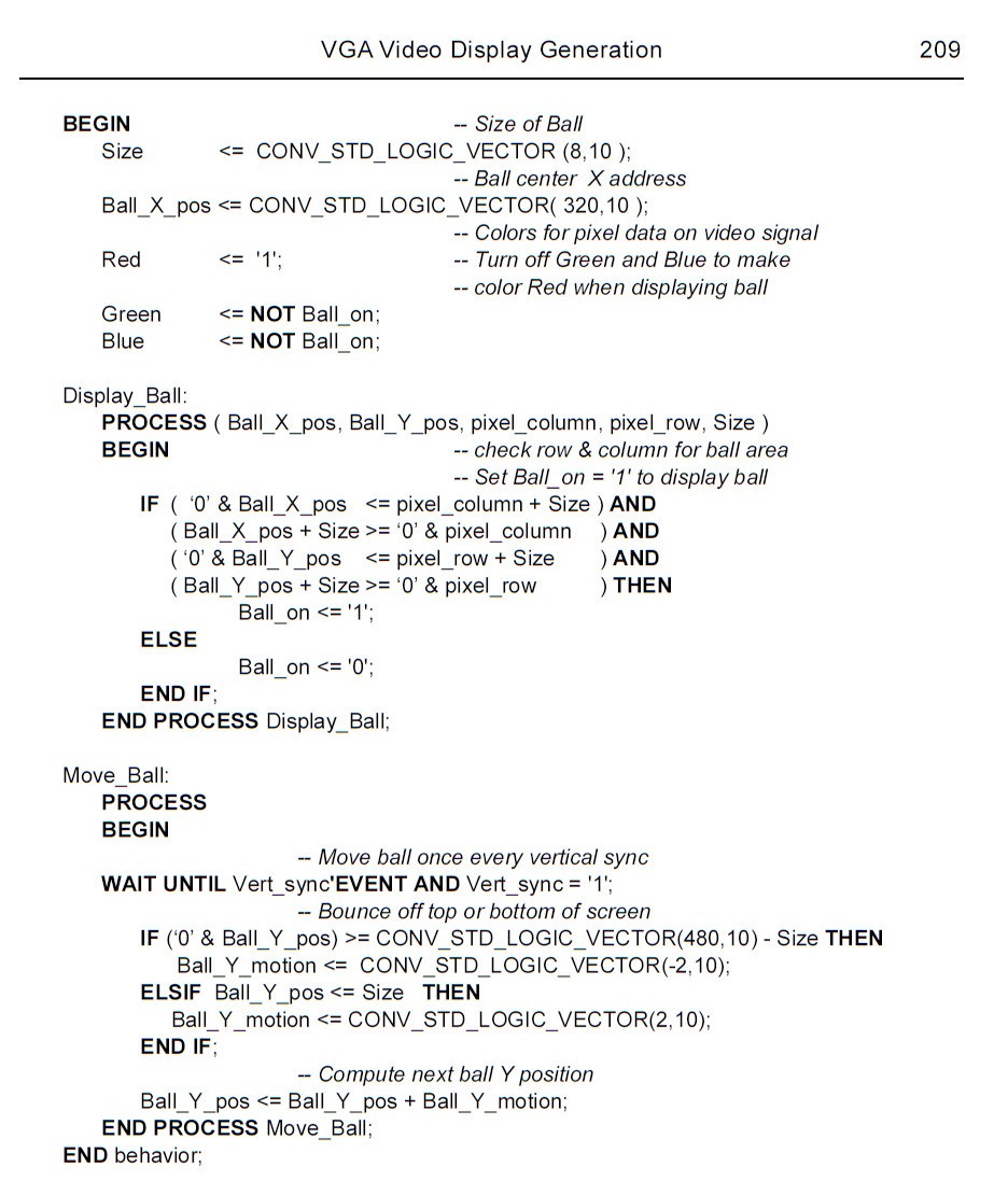
"BALL" Display PROCESS Example - VHDL Block #7
"PADDLE #1" Display PROCESS Example - VHDL Block #8 & #9
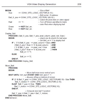
Also review pages 208 and 209 from the Accompanying Textbook I mentioned earlier.
The "RGB" Concatenation & Display Block
This Block is simply a group of "AND" gates that joins or "CONCATENATES" all of the RGB colors together into one MASTER RGB Output.
So you essentially have a Multi-Input "AND" gate for each of the individual RGB Colors. One for all of the RED colors, one for all of the GREEN, and one for all of the BLUE. Finally this MASTER RGB output can only be active during the Horizontal Display Time "AND" the Vertical Display Time. So yet another "AND" gate is used activate the MASTER RGB output only when H-DISPAY_TIME & V-DISPLAY_TIME are in a Logic HIGH state.
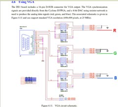
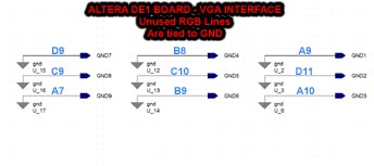
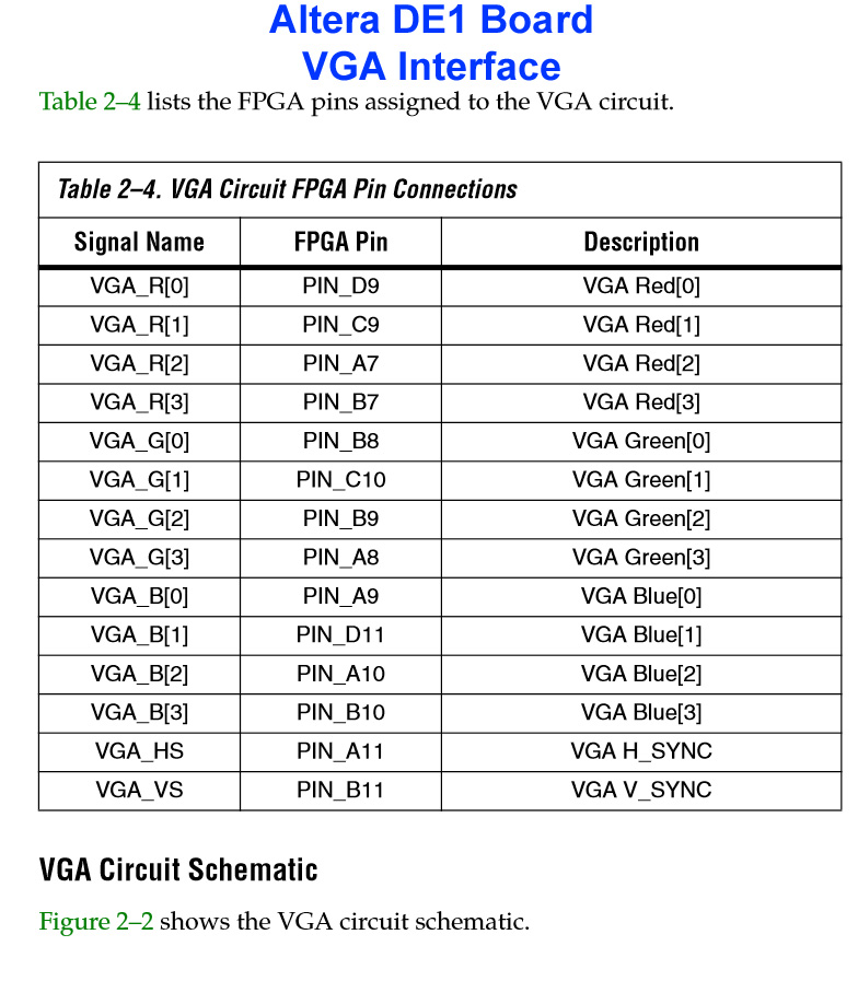
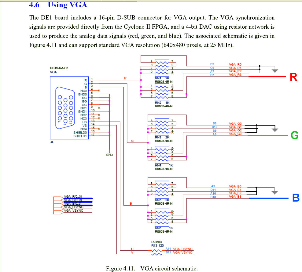
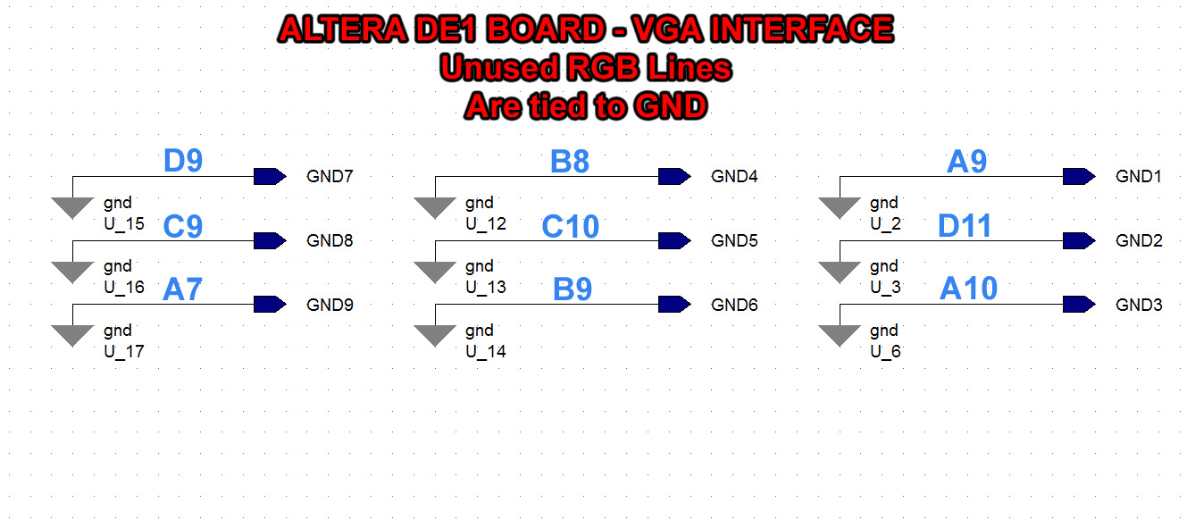
Altera DE1 Board - Unused RGB lines must be tied to GND.
It is important to make sure that you tie any unused RGB input lines to GND. As these can sometimes cause the unconnected signals to Float, producing interference and noise on your VGA monitor.
Well that about sums it up. :)
Hopefully this Tutorial will at least get you a little closer to finalizing your VHDL PONG Projects!
Fun Stuff!!
Cheers Folks!
-Gerry
-= END =-


