|
Current Time:
|
|
|
Gerry's Messy Electronics/Robotics Click the button below to go Back to the "CHIPPERY " section of my Lab
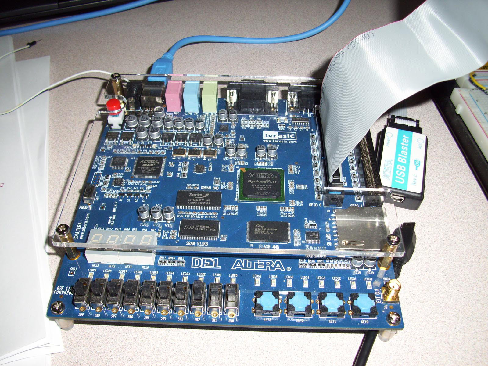
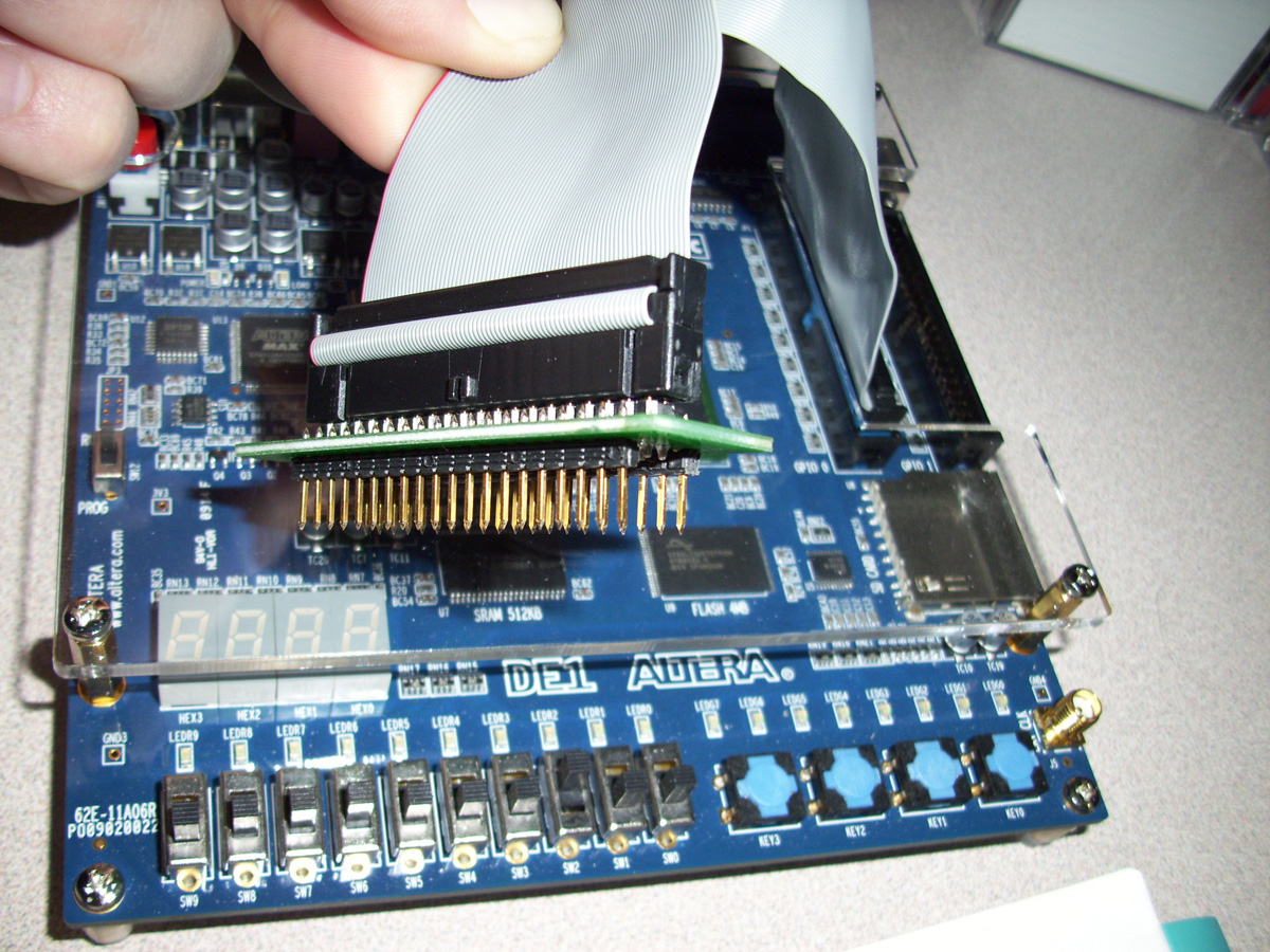
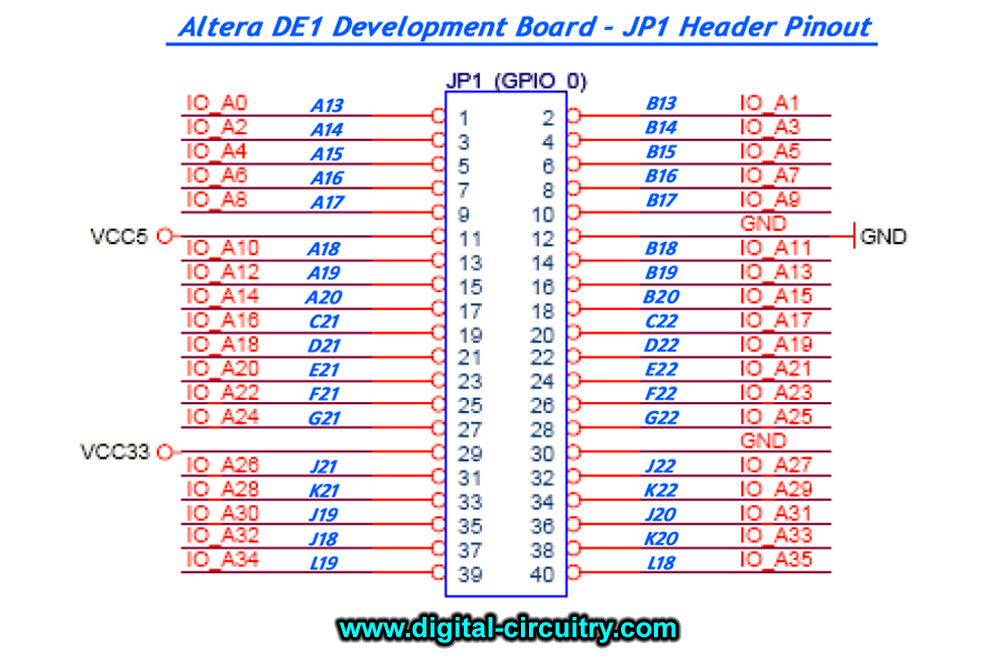
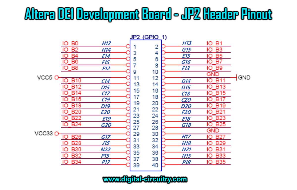
Altera DE-1 Development Board Shown below are some handy IDC Header pinout diagrams for the DE1 Board I made up. I have conveniently labeled each Pin with its appropriate FPGA pin designator. This is especially handy when you are assigning the FPGA Pins to your Logic design within your Logic design Software. If you are using this board for development projects in College or University, this is a big time saver. However, this is also Handy if just for your own digital labs at home. It saves having to spend extra time looking through the DE1 Reference Manual. The DE1 has two IDC Ribbon cable ports for interfacing purposes. They are referred to as JP1 & JP2 "Header" ports. This allows you to interface projects to external components on a breadboard using a IDC cable breakout adapter as shown in the image below. The adapter plugs into your breadboard like any other DIP intergrated IC, and provides interface connections that the DE1 Cyclone II FPGA can interface to, providing you with lots of interfacing possibilities.
Download links for the Altera DE1 User manuals and Full Development board Schematics are posted below.
If you're into the older Altera CPLD's you can Join my Altera Yahoo Group: http://groups.yahoo.com/group/AlteraMAX7000/
|
||
|
||

