-= Gerry's MENTOR GRAPHICS - HDL Designer Help =-
"COMPONENT Blocks -=VS=- VHDL Blocks"
There are several ways of implementing your design within HDL Designer, to makes things simple I will explain the method I have learned and has served me well. Just remember this is only one of many ways.
A "COMPONENT" has its own "Symbol Interface" and its own "Block Diagram" for holding Interconnections and logic Design Blocks. The Block Diagram for each Component holds the Logic makeup for that component specifically.
A VHDL Block is simply a Devoted code entry form, that is to be place within a Block Diagram of a Component.
Essentially this "COMPONENT" Feature is there to help provide structure to your Overall design. This helps keep your Circuit Organized allowing you to have embedded Secondary components within your master circuit.
The way I have always done things in the past, is to choose and assign a single Component Block as my "MASTER" Component for the Entire Project. This MASTER Component will hold the Entire logic design for the project. As you can see in the Image below, my chosen MASTER Component is Entitled "VGA_SYNC" which has its own devoted "Symbol Interface" and "Block Diagram". You can also see all of the other Logic Blocks that have been added to the Project. In this case all of the Logic BLOCKS have been designated as VHDL code Blocks.
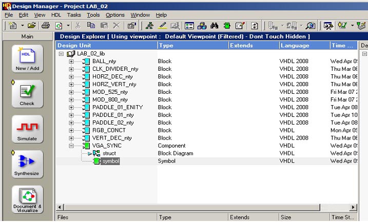
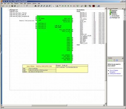
This MASTER Component "VGA_SYNC" is shown here below. This component will have its own sub-section "Symbol Block", which is essentially the components I/O interface Ports that are assigned to the Physical I/O Pins on the FPGA. There should be no interconnections on this MASTER Symbol page. You should only see your MASTER component (GREEN BLOCK) as it is seen here in the Image below. All additional design Blocks and interconnection for your design should be placed within the MASTER Block Diagram of this MASTER Component.
The MASTER Block Diagram is where you place all VHDL Blocks and other design blocks (Secondary Components if desired)
for your Project and you can interconnect them together.
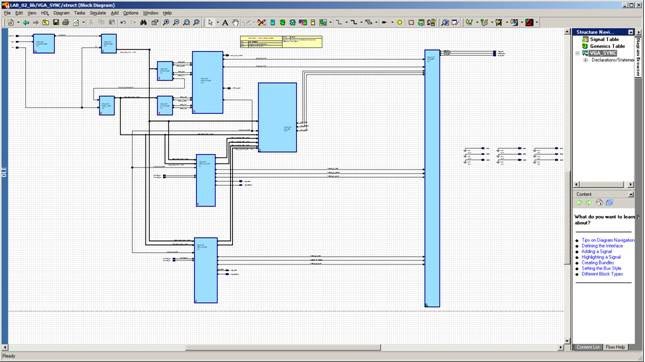
As seen here below within the "Design Manager" Window of HDL Designer, you can see my chosen MASTER Component is Entitled "VGA_SYNC" which has it's own devoted "Symbol" Interface and "Block Diagram". I use this Block Diagram to hold the entire design circuit for my Project.
So this becomes my "MASTER Component", "MASTER Symbol Interface" and "Master Block Diagram" circuit.
You can then have several Design Blocks of any kind (VHDL Blocks or even a Secondary COMPONENT Block) added to your project. Remember, all interconnections for these secondary components should only occur within your MASTER Block Diagram circuit.
So as an Example here below, my main Master Component and it's Block Diagram is the "VGA_SYNC" component.
I can create and add other secondary Components within the project, but I must only interconnect them within the MASTER Block Diagram of VGA_SYNC.
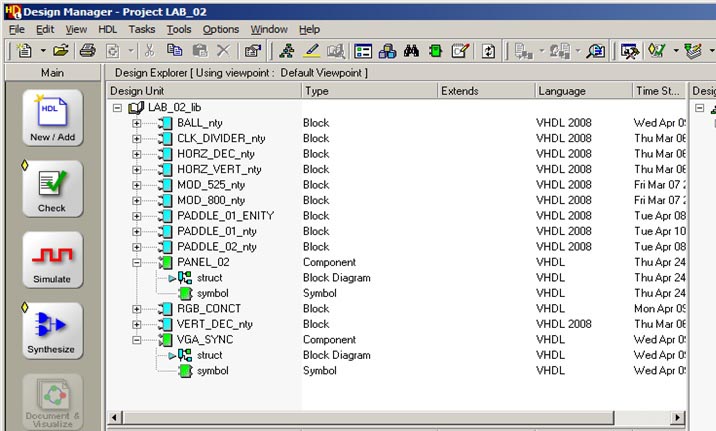
As you can see above, I have added the Component "PANEL_02" to the project which has it's own Symbol and Block Diagram which you can add Blocks to. However interconnections with this secondary Component itself as a whole, should only occur in the Block Diagram of VGA_SYNC. This is because VGA_SYNC is the chosen MASTER Block Diagram for the Project.
As you can see we place all Design Blocks (VHDL, etc.) and additional Component Blocks with their own devoted Block Diagrams,
within the MASTER Block Diagram Circuit.
As shown below:

So essentially you can have an infinite number of Components embedded within the Master Block Diagram Circuit.
When you think about it that's why they call it a "COMPONENT". It is a digital circuit of it's own design (Component Block Diagram) that is placed
on your Main Circuit Board (MASTER Block Diagram).
I hope this info will help solidify your understanding.
Cheers!
-Gerry
BACK TO MAIN PROJECTS PAGE
-PROJECTS-