I'm going to try and explain this in Layman terms in order to make sure you properly understand what is happening. Some of this may be basic knowledge to you, but it may not be for some other beginners. Regardless, have look at it and hopefully it will help solidify your understanding of how the Z80 Processor handles memory control and processing.
So here's the rundown on how it all works.
Below is a picture of the Pinouts for the All Mighty Nintendo Gameboy or SEGA GameGear's Z80 8-Bit Processor.
A whole wack load of pins there that might not be clear as to what the heck they are used for. Don't worry about that right now, just take a look at them and I'll try and explain their functions.
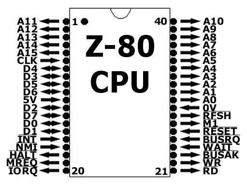
8-BIT DATA BUS
Essentially the way it works is that the Game consoles 8-BIT Z80 Processor has 8 pins on the chip reserved to send and receive Game Data (Pins entitled "D0" through to "D7").

So these are the wires that transfer all the information from the Connected Memory Chip and allows the Game to function the way it was designed to.
Combining these 8 wires together they essentially become what's called the 8-Bit “DATA BUS”. So the Z80 processor will only take in 8-Bits or 8 signals together at the same time.
This Parallel group of DATA Pins is called the "DATA BUS".
ADDRESS BUS
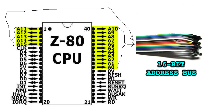
Now notice the Address Lines... on the Z80 Processor there are 16 of them. Entitled "A0" through to "A15".
These Address lines are used by the processor to essentially tell the Memory chip that it is connected to.....it will tell it which Storage location to open..... and read out whatever data is being stored in that location.
So the Address Lines are simply used to open and close a bunch of Storage "Drawers" and the Processor can either "READ" data from it, or "WRITE" (Store) data inside it for later access.
So that's what the Address Lines are used for....COOL!!!!
So when all of these address lines are grouped together they become the "ADDRESS BUS". Now the information stored in one of the Memory chips locations, it is up to the Game Designer during the programming process... what information to store in that particular Memory location. One location might be used to store some color information....and another for storing game scores. It's up to the Programmer where to store the data.
So the Z80 processor has 16 of these "Address Lines" available to send signals to the Memory chip that is inside the Game Cartridge plugged into the console. These Address lines are used to open and close many different storage locations to "READ" or "WRITE" data to.
Pretty cool. :)
BUS SIGNALS
So the way the signals work in the DATABUS & the ADDRESS BUS is this....
When the 16 Address lines are turned on or off in different binary patterns, it determines all the different "Drawers" so to speak....or memory storage locations in the memory chip that it can open. So 16 WIRES being tuned on or off in different sequences [0 volts or 5+ Volts] essentially represents a standard Binary pattern like "0000000011111111".
"0000000011111111" is a 16-BIT Binary number. Each BIT essentially represents one of the wires on the BUS. "0" represents when the wire for that BIT is at 0 volts. And a "1" represents when the wire is at 5+ Volts. This is the essence of Digital Signals used in Digital Electronics. So for the Z80's 16-BIT Address BUS delivering the Binary number "0000000011111111" this means that the first 8 wires (Represented by the RED Zeroes)....are at "0" volts, and the last 8 wires in Yellow....are at "5+" Volts. This Binary number essentially represents an Address to a specific "Drawer" or memory location inside the Memory chip. Just like numbers on Hotel Room Doors, a different number means a different room. Now you have to realize that each of these location in the memory chip can only store an 8-BIT binary number.
So once The Z80 processor opens a Memory location, the "DATA BUS" PINS on the Z80 processor will have direct access to this location. The DATA BUS pins literally peak inside to the opened memory location, and if an 8-BIT number has been stored there, it will READ it and send the 8-BIT number back to the Z80 processor over the DATA BUS for processing.
This means that each storage location inside the Memory Chip can only hold an 8-Bit Number inside it... like “0011 1010”, because the processor can only read and write data that are 8-Bits wide like “0011 1010” because it only has 8 wires to read 8 different Bits using its 8-BIT DATABUS pins. Get it?
This is why it's called an 8-BIT PROCESSOR!! TADA!!
COOL!!
The data which is stored in an 8-BIT memory chips location... will always be an 8-Bit Binary number like “0011 1010” because we are using an 8-Bit Processor.
So regardless of what the Processor wants to do with this Memory location….it can call up that location when it wants and "WRITE" DATA to it….or "READ" DATA from it. This is the function of the /WR and the /RD lines. So really....look at the ADDRESS lines as a way of numbering a whole wack load of storage Drawers. These "DRAWERS" or memory locations can hold game data inside them.
***8-Bits of data per Drawer ONLY! Please!!! *****
So let say we decide to use ATMEL's "AT49F040" 4MBit memory Chip and connect it to the Z80 Processor. This is essentially 4MBits of memory which = 512KB size ROMs game files. Remember this memory chip has A0 through to A18 Address Lines …… or 19 Address lines in total counting for the "A0" line.
19 Address Lines!! This is More ADDRESS LINES than the Z80 Processor has Right!! Your probably saying..."how does that work?". I’ll explain further down….keep reading.
So picture the whole 512KB (4Mbits) of the GAME ROM data, being broken up into equal blocks that will then be stored into various Storage locations. Remember, each of these locations inside the memory chip are numbered by the Binary patterns the Address lines create.
So the First address memory location for the AT49F040 would look like this:
0000000000000000000 (19 Zeros here)
The next storage location number would be :
0000000000000000001
And then:
0000000000000000010
Now don't get scared by the weird patterns of 1's and 0's in the numbers below. The important thing to realize is that each Binary number is different from the next. Check them out.
Now you can see the Binary Pattern forming ....and each number is different from the next.
0000000000000000011
0000000000000000100
0000000000000000101
0000000000000000110
0000000000000000111
0000000000000001000
0000000000000001001
0000000000000001010
0000000000000001011
0000000000000001100
0000000000000001101
0000000000000001110
0000000000000001111
0000000000000010000
So these are just a bunch of different numbers that are used to Label a Memory location, again like numbers on Hotel Room Doors. That's it! The real important Game DATA is what is being stored inside of these Memory locations. This important Game DATA is going to be sent over the DATA BUS to the Z80 for processing.
Now to make it easier for us to Read while looking at the data on our Computer monitors......these Long ass Binary numbers of 1's and 0's can be Converted into HEXADECIMAL numbers that are shorter and easier to read. They represent the same Binary number if you convert it back to Binary, but it just makes it easier for us when we are programming the game or just simply looking at it on the monitor. Hexadecimal numbers end up looking like this $FF80 or $FFFF. The “$” simply indicates that this is a “HEX” number.
If you convert "1111111111111111" to HEXADECIMAL it looks like this "$FFFF". This is definitely shorter and easier to read and remember than a long ass stream of 1's and zero's right!
Hexadecimal is just a shorter way of writing these long Binary numbers in order to make our lives easier.
COOL!!!
So, now using the ADDRESS LINES the Z80 has a whole Vault of storage locations that it has complete control over for storing the precious Game data.
The Processor can access each Storage "drawer" (memory Location) on command whenever it needs to…….and so when it needs a specific piece of DATA….. it will send a number out to the ADDRESS LINES that are connected to the Memory chip.
This will open that Storage location and expose the 8-Bits of GAME DATA Stored inside that location so it can read it or store some new Data to that location…… The DATA travels to or from the Z80 processor over the 8-BIT DATA BUS.
Remember!! The Z80 can only Read or Write 8-Bit Binary Numbers because it is limited to only 8 wires on it's DATA BUS.
More "ADDRESS LINES" means MORE MEMORY STORAGE LOCATIONS
With each added Address line you double the amount of Storage locations for storing DATA.
So with the Z80 processor itself, the maximum amount of memory locations it can control for storing Game Data... is all the various numbers it can create with its 16 ADDRESS LINES is "1111111111111111" which = 65,536 different Storage Drawers for storing 8-Bit numbers.
65,536 Memory locations, each holding an 8-BIT number you get:
65,536 X 8-Bits = 64 KiloBytes of Precious Game DATA.
This is because it only has 16 ADDRESS LINES (or a 16-Bit Address Bus).
1111111111111111 = 65,536 different Storage Drawers for storing different 8-Bit numbers.
Not too bad, but you would be surprised how fast this fills up. So what do you do when you need more Storage locations to have access to more Dame Data??
Here is where the "Memory Bank Controller" Chips come into play. :)
"MEMORY BANK CONTROLLER" & MEMORY "MAPPER" CHIPS
The Z80 combined with an "MBC" chip or "MAPPER" chip, you increase the number of Address lines you can use
(THIS IS THE MAIN PURPOSE OF THE MBC/MAPPER CHIP!!)
- With 17 ADDRESS Lines….. you get double the memory of that with 16 ADREESS Lines.
So 64KB x 2 = 128KB.
- With 18 ADDRESS Lines…..you get double that you get if you were using 17 ADDRESS Lines.
So 128KB x 2 = 256KB.
- With 19 ADDRESS Lines…..you get double that with 18 ADDRESS Lines.
So 256KB x 2 = 512KB.
So 20 Address Lines = 1Mbyte
21 Address Lines = 2Mbytes
22 ADDRESS Lines = 3Mbytes
23 ADDRESS Lines = 4MBytes
Also, don’t forget that the Address Lines usually start with "A0" so your Last Address Line is one less of the actual number of lines you are using.
Address Lines “A0 through to A22” is really 23 Address Lines. So having a 4MByte ROM or 32MBIT ROM you absolutely need to use the A0 through to A22. So this is an important thing to remember if you are designing a circuit.
Now, from the Z80’s Perspective….. with its Limited 16-Bit Address Bus……as I mentioned before, there are
65,536 Memory locations, each holding an 8-BIT number. So this means:
65,536 X 8-Bits = A MAXIMUM of 64 KiloBytes of Precious Game DATA
that we can access using the Z80 processors 16-BIT Address BUS.
Now out of all of these Thousands of Memory location numbers... Technically there are specific Locations or ADRESS LOCATION Numbers that are reserved for specific things and they can not be used for storing Game data into Memory.
Usually each Game System will have its own set of guidelines on how the system will function and where specific pieces of information should be stored.
This is usually referred to as the Processors “MEMORY MAP”.
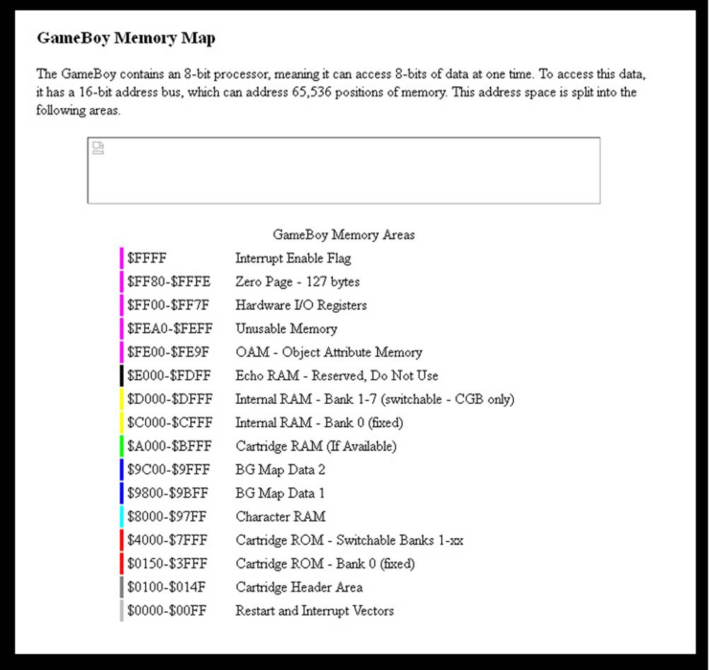
The Gameboy’s Z80 Processor MEMORY MAP is shown Below:
Following is a memory map of the SMS/GAME GEAR:
| Address |
Contents |
Size |
| $0000-$00ff |
ROM |
1KB |
| $0100-$3fff |
ROM (slot 1) |
15KB |
| $4000-$7fff |
ROM (slot 2) |
16KB |
| $8000-$bfff |
ROM (slot 3) |
16KB |
| $c000-$dfff |
RAM |
8KB |
| $e000-$ffff |
RAM (mirror) |
8KB |
Memory Locations FFFCh through to FFFFh and DFFCh-DFFFh are for interfacing to the Memory Mapper.
The "MBC" chip or a "MAPPER" chip essentially will handle a big chunk of the storing and retrieving of the data in a more controlled manner and using some clever Logic trickery in Digital Circuitry design…….
With this added component, the Z80 Processor can manage to Map out Larger Memories using only it’s 16-Bit Address BUS……....with the help of the MBC/MAPPER chip of course.
So this is the Purpose of the MBC chip and that’s why it’s called “MEMORY BANK CONTROLLER”.
And this is why whenever people are talking about the Z80 Processor itself, and how it handles memory…..they talk about its 16-Bit Address Bus.
However….when it comes to the Z80 processor partnered with the MBC or MAPPER chip….. it now has a 19-Bit Address Bus….. or higher. :) Depending on the MBC chip you are using.
-=END=-
This is a lot to take in at once.... and so you may need to read this a few times before getting it all.
If you want me to continue even Deeper with more explanations, send me an email and I will update this with more information on the other Z80 PINs. :)
I hope this was able to help you understand some of the 8-BIT Memory Interfacing concepts.
Cheers!
-Gerry